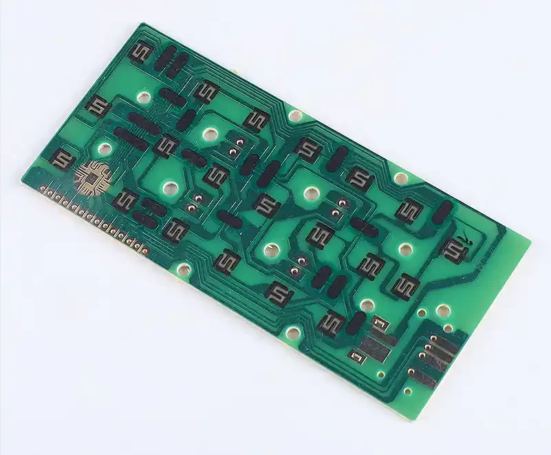
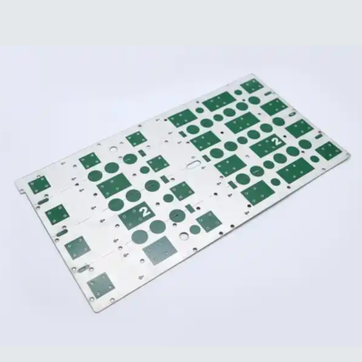
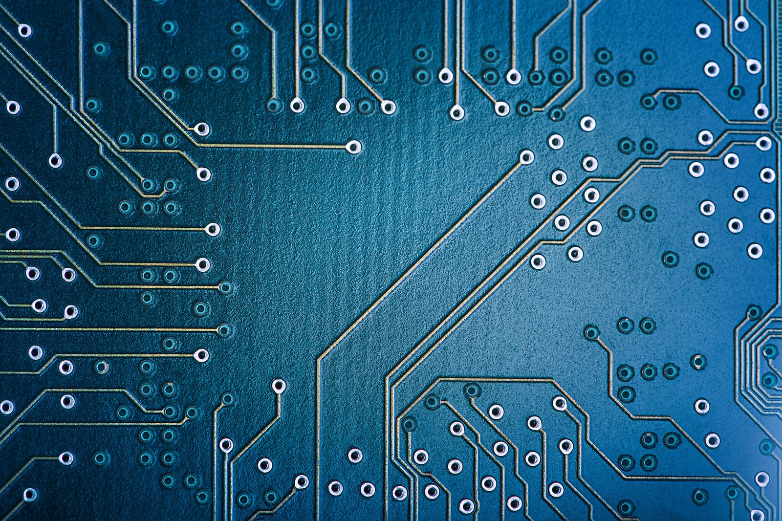
Single-layer PCB in MultPCB
High-Quality Single-Layer PCBs for Your Simplest to Complex Needs!
What is a Single-Layer PCB and Why Use it?
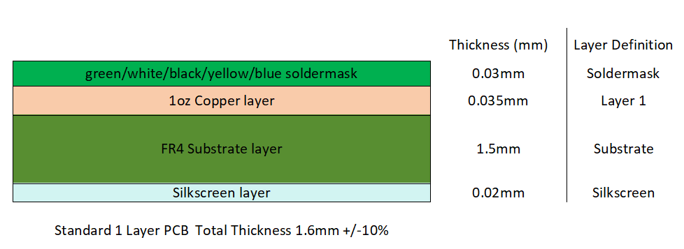
“Single-Layer PCB (Printed Circuit Board), also known as a Single-Sided PCB or a one layer PCB, is the simplest type of PCB. It consists of only one conductive layer of copper that is mounted on a single side of a substrate material, such as FR1, FR4, CEM-1, CEM-3, aluminum-based, copper-based etc. The other side of the substrate is typically used for mounting components, leaving the conductive layer for electrical connections.”
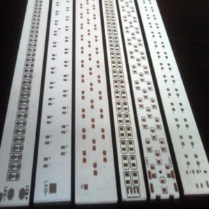
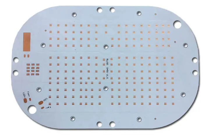
“Single-Layer PCBs are cost-effective and perfect for some simple electronics. They are ideal PCB boards for products like calculators, power supplies, and LED lighting etc.”
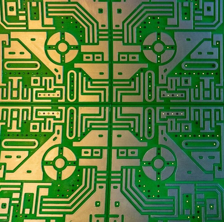
Standard Single-layer PCB Stack-up Structure
Advantages and Disadvantages of Single Sided PCB
Advantages:
• Cost-effective
• Simple design and manufacturing
• Quick turnaround
• Compact size
• High reliability for simple applications
• Easier testing
• Lower power consumption for specific applications
Disadvantages:
• Limited component density
• Limited design complexity
• Space constraints
• Limited routing complexity
• Increased size for complex designs
• Lack of high-speed signal integrity
• Limited applications in advanced electronics
MultPCB 1-layer PCB Capabilities
| Capability | Details |
| Substrate Material | FR1, FR4 (fiberglass epoxy), CEM-1, CEM-3, and Metal Core (for heat dissipation applications). |
| Copper Thickness | Half oz/ft² (0.018mm), 1 oz/ft² (0.035mm), 2 oz/ft² (0.070mm), 3 oz/ft² (0.105mm) |
| Board Thickness | 0.2mm to 3.2mm |
| Solder Mask Color | Green (standard), also available in red, blue, black, yellow, white colors |
| Surface Finish | HASL (Hot Air Solder Leveling), ENIG (Electroless Nickel Immersion Gold), OSP (Organic Solderability Preservative), and immersion tin for enhanced solderability. |
| Silkscreen | White and Black color |
| Drilling | 0.3-6.5mm |
| Impedance Control | YES |
| Minimum Trace Width | 4 mils (0.1mm) |
| Testing | Comprehensive testing options including AOI (Automated Optical Inspection), E-test, and Flying probe test |
| Lead Time | Fast turnaround 1-5days, Standard 5–7 days, volume order 8-15 days depend on quantity |
| Application Areas | simple electronic devices like power supplies, LED lighting, consumer electronics, automotive sensors, and more. |
| Component Mounting | Surface Mount Technology (SMT) and Through-Hole Technology (THT) |
How to Produce A Single-sided PCB?
The production of a Single-Sided PCB involves several key steps that ensure the board is properly manufactured, functional, and ready for component assembly. Below is a step-by-step guide on how to produce a single-sided PCB:
Steps | Description |
Design and Layout | Create a schematic and layout; generate Gerber files. |
Material Selection | Choose substrate (FR4), copper foil, solder mask, and silkscreen material. |
Printing PCB Design | Apply photoresist and expose to UV light to transfer design to the copper layer. |
Etching | Remove unwanted copper to form the traces and pads. |
Drilling | Drill holes for components or vias. |
Solder Mask Printing | Apply and cure the solder mask to protect traces. (Green, Yellow, White, Black, Blue, Purple) |
Silkscreen Printing | Print labels, component markings, and logos. ( Black and White) |
Surface Finish | Apply surface finish to copper pads (HASL, ENIG, OSP). |
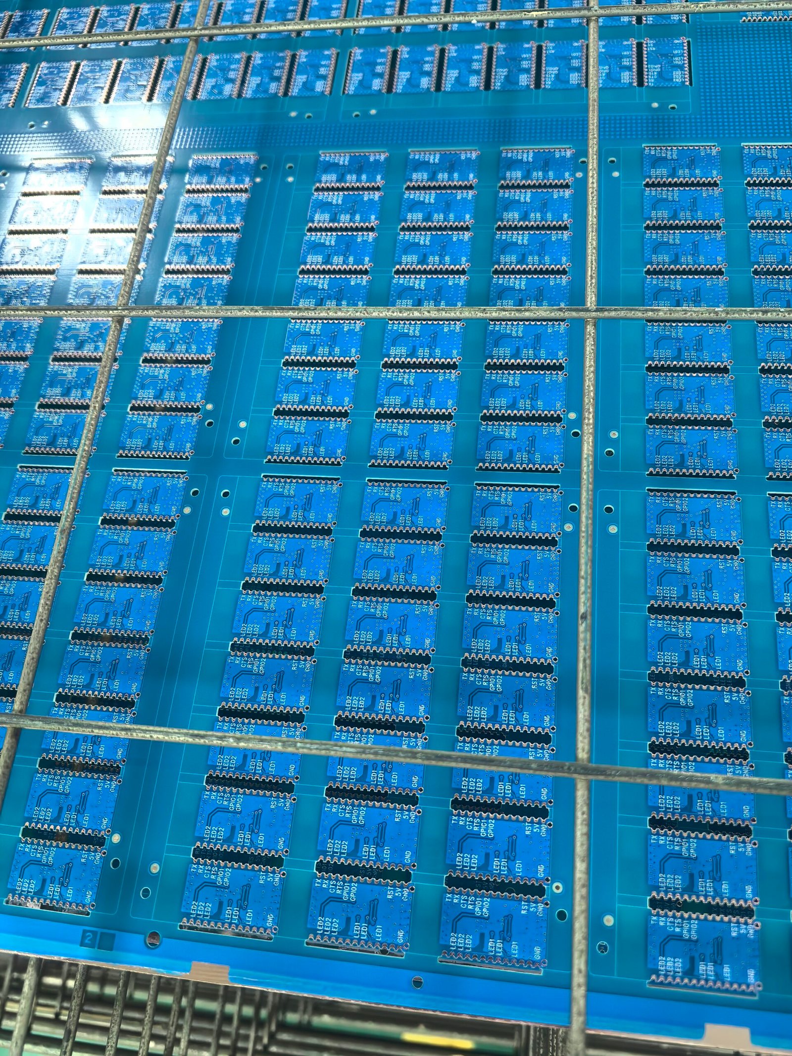
Profiling and Cutting | Cut the PCB to its final shape and size. (Panel and single piece form) |
Electrical Testing | Open and short circuits testing |
Inspection and Packaging | Inspect the final PCB boards, clean it, and prepare for shipment. |
This is the general process used to manufacture a single-sided PCB. The steps might vary slightly based on the specific requirements of the design or the manufacturer, but the core process remains the same.
Applications of single layer PCB
Key Features of Single-sided PCBs:
- Simple Design Requirements
- Low Cost
- Compact Size
- Reliability
Single-layer PCBs (also known as single-sided PCBs) are widely used in various industries due to their simplicity, cost-effectiveness, and reliability for straightforward circuit designs. Below are the key applications of single-layer PCBs:
* Consumer Electronics
Such as calculators, remote controls, coffee machines, and small kitchen appliances.
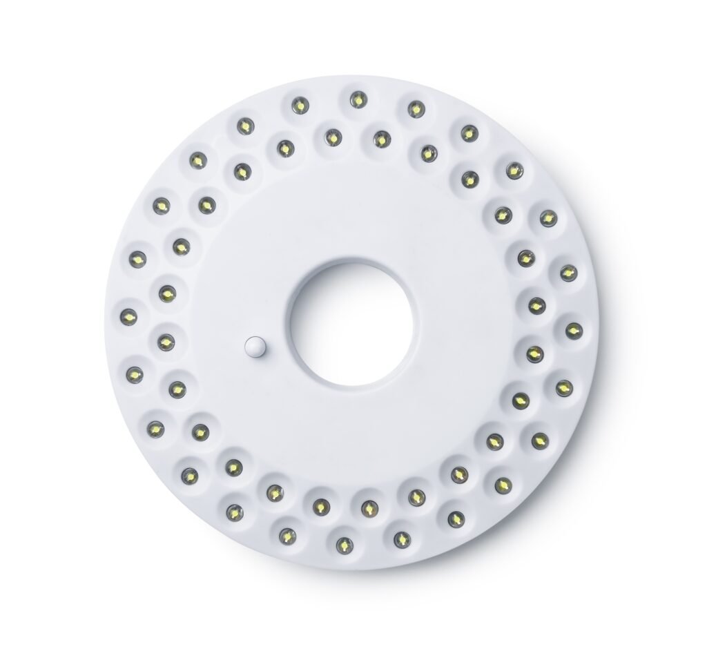
* LED Lighting
Such as LED bulbs, lighting strips, and decorative lighting solutions.
* Automotive Electronics
Such as dashboard indicators, headlight systems, and wiper controls.
* Power Supplies
Such as chargers, adapters, and power banks.
* Industrial Equipment
Such as relays, power converters, and sensors.
* Medical Devices
Such as blood pressure monitors, glucose meters, and hearing aids.
* Home Appliances
Such as washing machines, air conditioners, and refrigerators.
* Audio and Visual Equipments
Such as speakers, amplifiers, and DVD players.
* Toys and Hobby Electronics
Such as electronic toys, educational kits, and DIY
* Security Systems
Such as doorbells, motion detectors, and simple alarms.
Single-layer PCBs are an excellent choice for applications where advanced circuit complexity is unnecessary, and cost efficiency is a priority.
Why order single-sided PCB from MultPCB?
- Assurable CCL(Copper-clad Laminate) from Brand supplier, such as KB, Shengyi, ILM, Nanya Etc;
- High automatic production line ensure good quality
- Low and competitive price
- No MOQ, you can order 1pcs to 1000k pieces per order
- Quick-turn Production, 1-3days for sample, 10-15 days for volume order;
- After-sale service