Multilayer PCB in MultPCB
Discover our expertise, advanced capabilities, and why our multilayer PCBs stand out in today’s competitive market.
At MultPCB, our multilayer printed circuit boards are designed for the most demanding applications—providing unparalleled performance, reliability, and design flexibility. Our advanced manufacturing process ensures precise interconnections and exceptional signal integrity for your high-speed and complex circuits.
What Is a Multilayer PCB?
A multilayer PCB is a sophisticated circuit board that consists of three or more layers of conductive traces separated by insulating layers. This design allows for:
High-Density Interconnections: Multiple layers enable complex routing and compact designs.
Enhanced Signal Integrity: Reduced electromagnetic interference (EMI) and controlled impedance for high-frequency applications.
Compact Form Factor: Ideal for advanced consumer electronics, telecommunications, medical devices, and automotive applications.
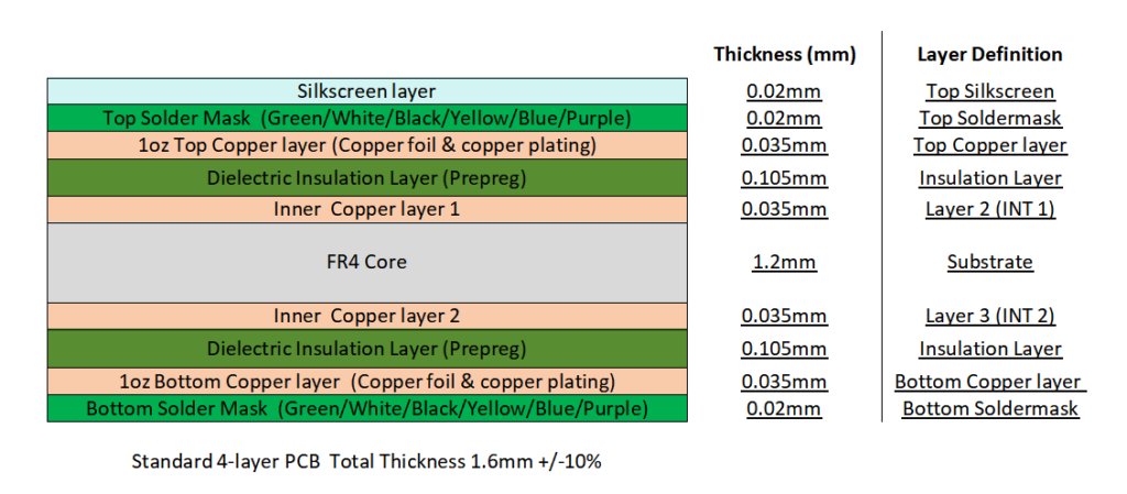
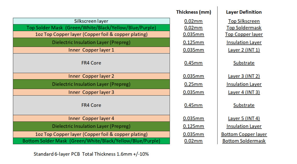
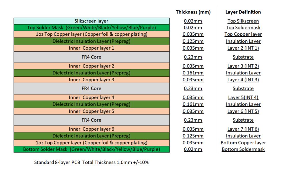
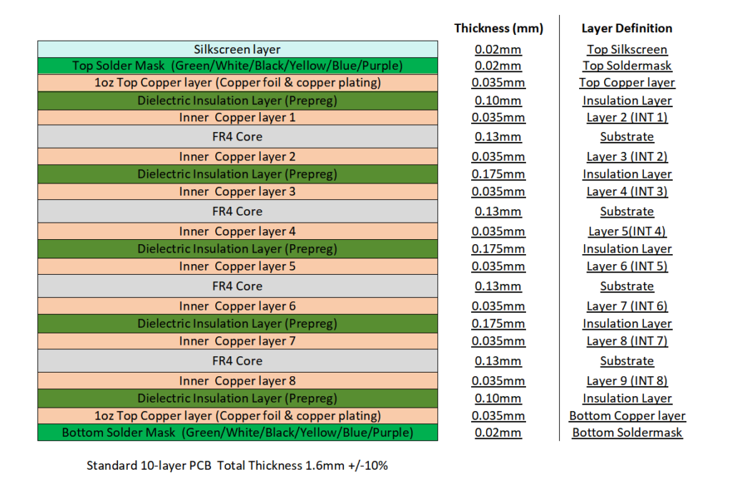
Standard Multilayer PCB Stack-up Structure
Below you can see the stack-up structure of :
- Standard 4-layer PCB
- Standard 6-layer PCB
- Standard 8-layer PCB
- Standard 10-layer PCB
These diagrams provide a comprehensive overview of the typical lamination structure for multilayer PCBs from 4 to 10 layers. Feel free to contact us if you need further customization or technical support for your specific project requirements.
Actually for multilayer PCB, the overall thickness can be varied as 1.6mm, 1.8mm, 2.0mm, 2.4mm or higher according different stack-up structure, and the thickness tolerance is+/-10% per IPC class 2 standard.
Standard 4-layer PCB Stack-up Structure
Standard 6-layer PCB Stack-up Structure
Standard 8-layer PCB Stack-up Structure
Standard 10-layer PCB Stack-up Structure
Why order Multilayer PCB from MultPCB?
At MultPCB, we leverage decades of industry expertise to deliver high-quality multilayer PCBs. Our key advantages include:
Precision Manufacturing: State-of-the-art equipment and tight process control guarantee accuracy and consistency.
Advanced Material Options: We use premium-grade substrates and high TG materials to meet diverse performance needs.
Expert Engineering Support: Our experienced team collaborates with you from design to production, ensuring an optimized solution for your application.
Timely and fast response: Once there’s any inquiry or quesetion from customer, our team is very responsive and can reply in same day.
Rapid Turnaround: Efficient production and quality control processes allow us to deliver on schedule, even for complex, high-layer count boards.
Competitive Pricing: Streamlined processes and volume capabilities ensure cost-effective solutions without compromising quality.
Multiayer PCB Capabilities at MultPCB
At MultPCB, we offer comprehensive multilayer PCB manufacturing capabilities tailored to meet diverse project requirements. Below is an overview of our multilayer PCB capabilities:
| Feature | Details |
| Base Materials | FR4, High-Tg FR4, Halogen-Free FR4 |
| Layer Count | Up to 32 layers |
| Board Thickness | 0.6mm – 3.2mm |
| Copper Thickness | 0.5oz – 6oz |
| Surface Finishes | HASL (Lead & Lead-Free), ENIG, Immersion Silver, OSP |
| Min. Line Width/Spacing | 3mil/3mil |
| Min. Drill Hole Size | 0.15mm |
| Solder Mask Colors | Green, Blue, Black, White, Red, Yellow |
| Advanced Features | Blind/Buried Vias, Gold Fingers, Press Fit Holes, Via-in-Pad Technology |
| Testing Methods | Automated Optical Inspection (AOI), Electrical Testing (E-test, Flying Probe Test) |
| Lead Times | Prototype: 3-8 days; Standard: 7–12 days; Volume Orders: 10-20 days, depending on quantity |
| Component Mounting | Surface Mount Technology (SMT) and Through-Hole Technology (THT) |
| Quality Certifications | ISO 9001, IATF 16949, UL |
| Applications | Consumer Electronics, Medical Devices, Aerospace, Telecommunications, Military, Automotive, Wearables, IoT |
How to Produce A Multilayer PCB at MultPCB?
Here is a detailed overview of the multilayer PCB manufacturing process presented in a tabular format:
| Step | Description |
| 1. Design and Output | Create the PCB layout using design software and generate manufacturing files such as Gerber files and Bill of Materials (BOM). |
| 2. Material Selection | Choose appropriate base materials like FR4, High-Tg FR4, or Halogen-Free FR4 based on performance requirements. |
| 3. Inner Layer Imaging | Transfer circuit patterns onto inner layer cores using photosensitive dry film and ultraviolet (UV) light exposure. |
| 4. Inner Layer Etching | Chemically remove unwanted copper from the inner layers, leaving only the intended circuit traces. |
| 5. Inner Layer Inspection (AOI) | Utilize Automated Optical Inspection (AOI) systems to detect defects in inner layers before lamination. |
| 6. Lamination | Stack inner layers with prepreg (insulating layers) and copper foil for outer layers, then bond them under controlled heat and pressure to form a unified multilayer board. |
| 7. Drilling | Drill holes for vias and component leads with high precision to ensure accurate layer interconnections. |
| 8. Plated Through-Hole (PTH) Process | Deposit a thin layer of copper inside drilled holes through a chemical process, establishing electrical connections between layers. |
| 9. Outer Layer Imaging | Apply photosensitive film to outer surfaces and expose them to UV light through a photomask, defining the outer layer circuitry. |
| 10. Outer Layer Etching | Etch away unwanted copper from the outer layers, preserving the circuit patterns. Remove the remaining photoresist to expose the final copper traces. |
| 11. Solder Mask Application | Apply solder mask over the board surfaces, leaving only designated areas (like pads) exposed for soldering. |
| 12. Surface Finishing | Apply finishes such as HASL (Hot Air Solder Leveling), ENIG (Electroless Nickel Immersion Gold), or OSP (Organic Solderability Preservative) to exposed copper areas to protect against oxidation and enhance solderability. |
| 13. Profiling and Cutting | Cut the PCB to its final shape and size. (Panel and single piece form) |
| 14. Silkscreen Printing | Print component designators, logos, or other markings onto the board surface for assembly and identification purposes. |
| 15. Electrical Testing | Perform tests like Flying Probe or Bed of Nails to verify electrical continuity and functionality of the PCB. |
| 16. Final Inspection and Quality Control | Conduct thorough inspections to ensure the PCB meets all specified requirements and is free from defects. |
| 17. Packaging and Shipping | Package the PCBs securely to prevent damage during transit and ship them to the customer. |
Please note that the above steps represent a general process for multilayer PCB manufacturing, specific manufacturers may have different procedures and sequences.
Applications of Multilayer PCB
Multilayer PCBs offer high-density interconnects and enhanced electrical performance, making them ideal for complex and high-speed applications. Here are some key application areas:
High-Speed Computing and Networking:
Multilayer PCBs are used in servers, data centers, and high-performance computing devices where signal integrity and controlled impedance are critical.Telecommunications and RF Systems:
They support advanced communication systems, including smartphones, base stations, and RF modules, by minimizing electromagnetic interference (EMI) and ensuring reliable high-frequency performance.Consumer Electronics:
From smartphones and tablets to laptops and gaming consoles, multilayer PCBs help achieve compact, densely packed designs with multiple integrated functions.Automotive Electronics:
Used in advanced driver-assistance systems (ADAS), infotainment systems, and power management modules, multilayer PCBs meet stringent reliability and performance requirements in harsh environments.Aerospace and Defense:
In these critical applications, multilayer PCBs are employed in navigation systems, radar, and communication equipment due to their robust construction and high signal integrity.Medical Devices:
Multilayer boards are essential in diagnostic imaging, portable medical equipment, and wearable health monitors, where reliability and precision are paramount.Industrial Control and IoT:
They are widely used in automation, robotics, and smart devices, providing the necessary interconnect density for complex control systems.
These applications demonstrate how multilayer PCBs are pivotal in driving innovation across various industries, enabling miniaturization, improved performance, and enhanced functionality.
FAQs About Multilayer PCB at MultPCB
1. What is a multilayer PCB?
Multilayer PCBs are printed circuit boards composed of three or more layers of conductive material separated by insulating layers. They allow for complex circuit designs with high interconnect density, improved signal integrity, and reduced electromagnetic interference.
2. What advantages do multilayer PCBs offer over single or double-sided PCBs?
They provide higher density interconnections, better electrical performance, and allow for more compact designs. This makes them ideal for high-speed, high-frequency applications and complex systems where space and signal integrity are critical.
3. What are the typical layer counts and board thicknesses for multilayer PCBs?
At MultPCB, we manufacture multilayer PCBs ranging from 4 to 32 layers. For example, a standard 4-layer board might have a total thickness of approximately 1.6mm, while our higher layer-count boards can vary from 0.6mm to 3.2mm, depending on design requirements.
4. What materials do you use for multilayer PCB production?
We use a variety of high-quality base materials, including standard FR4, high-Tg FR4 for improved thermal performance, and halogen-free FR4 for environmentally friendly solutions. Our material selection is based on the specific needs of each project.
5. What surface finishes are available for multilayer PCBs?
Our multilayer PCBs can be finished with several options, including HASL (both leaded and lead-free), ENIG, immersion silver, and OSP. Each finish is chosen to enhance solderability, prevent oxidation, and meet the end application’s requirements.
6. What is the typical lead time for multilayer PCB production at MultPCB?
For prototype orders, we can usually turn around production in 3-8 days. Standard production typically takes 7-10 days, while volume orders may require 8-20 days, depending on the complexity and quantity of the order.
7. What testing methods do you use to ensure multilayer PCB quality?
We utilize a range of testing and inspection methods including Automated Optical Inspection (AOI), electrical continuity tests (E-test), and flying probe testing. These methods help us detect any defects early and ensure that every board meets our high-quality standards.
8. Can MultPCB produce custom stack-up structures for multilayer PCBs?
Absolutely. We offer both standard and custom stack-up structures. Our experienced engineers work closely with you to optimize the layer configuration, materials, and overall design to meet your specific electrical and mechanical performance requirements.
9. What applications are multilayer PCBs typically used in?
Multilayer PCBs are essential in many high-performance applications such as high-speed computing, telecommunications, consumer electronics (like smartphones and tablets), automotive electronics, aerospace, medical devices, and industrial control systems.
10. How do I ensure my design is manufacturable for a multilayer PCB?
We recommend that you collaborate with our design team early on. We conduct thorough Design for Manufacturability (DFM) checks, provide feedback on layout optimizations, and ensure that your design specifications align with our production capabilities. This collaborative approach helps in minimizing errors and reducing time-to-market.