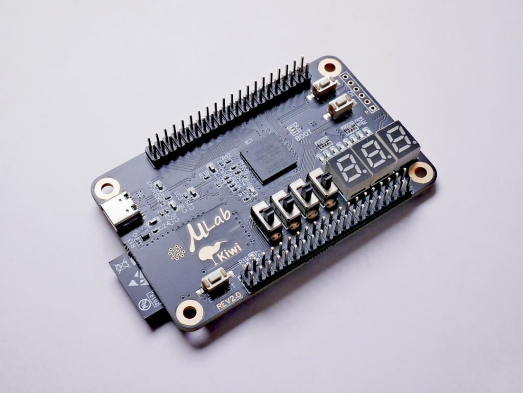
Printed Circuit Boards (PCBs) are the essential infrastructure of modern electronics, enabling functionality by routing electrical signals between components. This article delves into the detailed steps of PCB manufacturing, highlighting the precision and complexity involved in creating these vital electronic components.
Introduction to PCBs
What Are PCBs?
PCBs are thin boards made from non-conductive substrates layered with conductive copper traces. These traces form the electrical pathways that connect various components.
Why Are PCBs Important?
- Core of Electronics: PCBs are integral to nearly every modern device, from simple calculators to advanced medical equipment.
- Customizability: They support single, double, and multilayer configurations, enabling complex circuit designs.
- Durability: High-quality PCBs ensure reliable performance in various environments.
Overview of the PCB Manufacturing Process
The PCB manufacturing process involves 20+ steps that ensure the board’s precision, functionality, and durability. These steps encompass design, material preparation, layer creation, and rigorous quality checks.
Detailed Steps in PCB Manufacturing
Step 1: Design and Output
- Design Phase: Engineers create PCB layouts using software like Altium, Eagle, or KiCad. These designs must consider track width, spacing, and hole sizes.
- Export to Gerber Files: Designers export the layout in Gerber format, containing data on copper layers, solder masks, drill files, and other specifications.
- DFM Check: Fabricators conduct a “Design for Manufacture” check to ensure the design can be produced efficiently.
Step 2: Film Creation
- Plotter Printing: Special printers create photo films of the PCB layers.
- Black and Clear Inks: Black represents conductive areas, while clear denotes non-conductive zones.
- Registration Holes: Films are punched with alignment holes to ensure perfect layer alignment during production.
Step 3: Inner Layer Printing
- Cleaning: Copper laminates are cleaned to remove contaminants.
- Photo-Resist Coating: A UV-sensitive layer is applied.
- UV Exposure: The photo film is aligned with the laminate, and UV light hardens the desired areas.
- Development: Unhardened photo-resist is washed away, leaving copper traces as designed.
Step 4: Copper Etching
- Etching Process: Chemical baths remove unwanted copper, revealing the PCB’s conductive pathways.
- Inspection: Technicians verify the etched patterns for accuracy and defects.
Step 5: Layer Alignment and Optical Inspection
- Optical Punch: Ensures precise alignment of layers using registration holes.
- Automated Optical Inspection (AOI): Compares the layers against the design files to detect defects.
Step 6: Layer Bonding and Lamination
- Prepreg Layers: Layers of epoxy-impregnated fiberglass are placed between copper sheets.
- Stacking: The layers are stacked in sequence (inner core, prepreg, outer layers).
- Pressing: Heat and pressure bond the layers into a single structure.
Step 7: Drilling
- Drill Preparation: X-rays locate precise drill points.
- Drilling Process: Computer-guided drills bore holes for vias and mounting.
- Cleaning: Burrs are removed, and the drilled holes are inspected.
Step 8: Plating
- Chemical Bath: A thin layer of copper is deposited over the entire board, including the drilled holes.
- Purpose: This step creates conductive pathways between layers.
Step 9: Outer Layer Imaging and Etching
- Photo-Resist Application: Re-applied to outer layers.
- UV Imaging and Etching: Similar to inner layers, this step defines the outer layer’s copper traces.
Step 10: Solder Mask Application
- Protective Coating: Solder mask is applied to shield copper traces from oxidation and damage.
- UV Hardening: Ensures the solder mask adheres to the board.
Step 11: Surface Finish
- Types of Finishes:
- Immersion silver for low signal loss.
- ENIG (Electroless Nickel Immersion Gold) for durability.
- HASL (Hot Air Solder Leveling) for cost-effectiveness.
- Purpose: Protects copper traces and improves solderability.
Step 12: Silkscreen Printing
- Markings: Adds labels, part numbers, polarity markers, and logos to the PCB.
- Methods: Inkjet or laser printing for precision and clarity.
Step 13: Electrical Testing
- Continuity Tests: Ensure no open circuits.
- Isolation Tests: Verify no short circuits exist.
- Advanced Testing: Flying probe tests check each net on the bare board.
Step 14: Profiling and Scoring
- Routing Out: Boards are separated from the production panel using CNC routers or V-grooves.
- Edge Finishing: Ensures smooth and burr-free edges.
Special Considerations for Multilayer PCBs
- Inner Layer Imaging and Etching: Similar to single-layer processes but repeated for multiple layers.
- Oxide Application: Enhances adhesion between layers.
- X-Ray Alignment: Ensures precise drilling for interlayer connections.
Final Quality Inspection and Packaging
- Visual and Dimensional Checks: Ensure compliance with design specifications.
- Protective Packaging: Boards are vacuum-sealed to prevent dust and damage during transit.
Conclusion
The PCB manufacturing process is a meticulous and highly controlled series of steps. From design to testing, every stage ensures the board meets strict quality and performance standards. By partnering with experienced manufacturers, you can guarantee reliable, durable, and high-quality PCBs for your projects.
This comprehensive process reflects the precision and expertise required in the creation of these foundational electronic components.


